
Back to PCB Design With AI Doing the Legwork: An NFC Business Card in KiCad
$ grep -n "^##" 2026-10-ai-assisted-pcb-design-kicad-nfc-business-card.mdx
I used to design circuits and lay out boards in KiCad, order them, and do my own surface-mount assembly. I still want to build electronics; I have less time. So over 24–26 October 2026 I ran an experiment: let coding agents do the research, sourcing, file generation and iteration for a small board while I reviewed decisions and outputs. The board is a business-card-sized NFC tag that a phone's field powers and that answers with a profile URL. It went through three native KiCad revisions, the last adding a field-powered LED, plus five art studies.
The result is an editable KiCad project set with clean native checks and a manufacturing package. Nothing has been fabricated or measured. The honest claim is narrower than the renders: AI made it practical to produce and iterate on inspectable design artifacts, but the confidence came from datasheets, exact part identities, assembly rules, native checks and independent examination, not from a plausible picture.
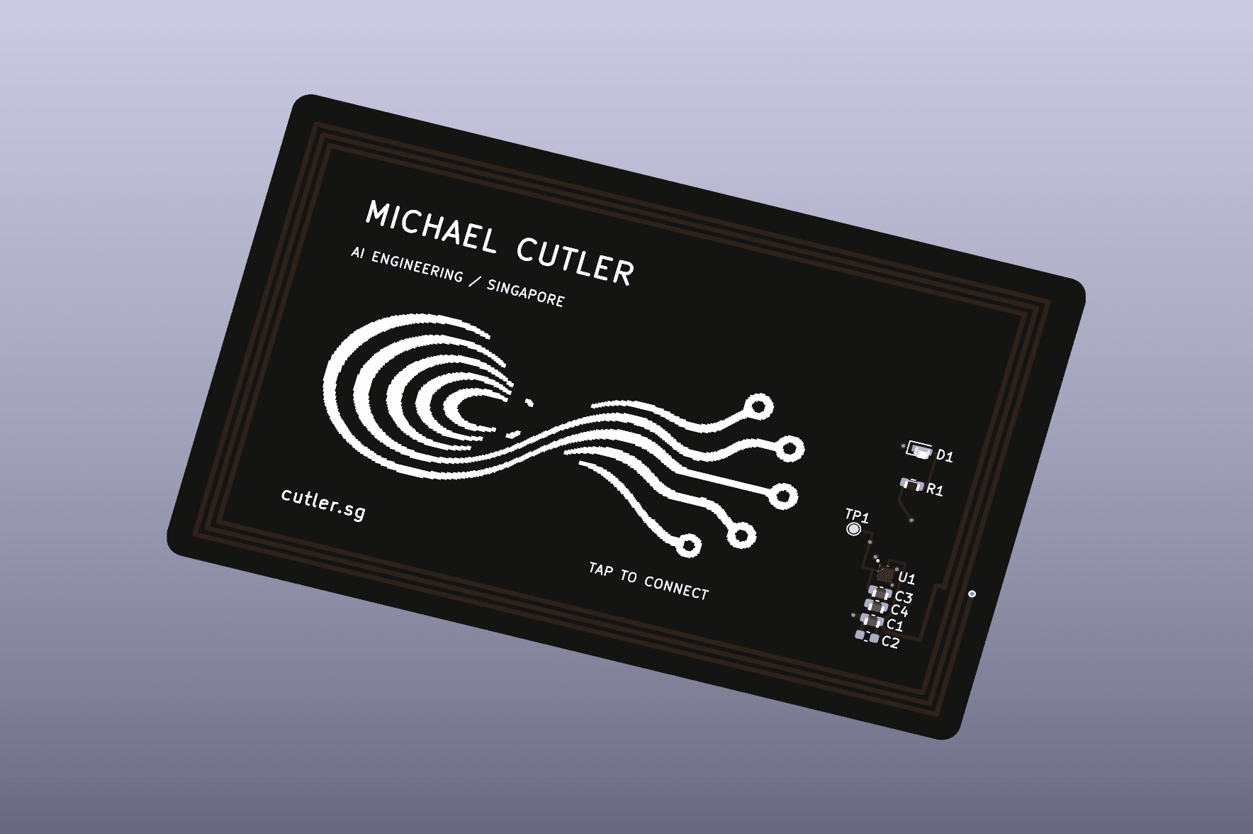
The board, and where the idea came from
The inspiration was a 2019 Instructables project, PCB Business Card With NFC, which used an NXP NT3H1101 and a PCB-trace loop antenna on a card. Inspiration only: its page body extracted poorly, its licensing was never established, and nothing was copied. The design here was generated independently and is not a validated reproduction.
The brief: card format, 85 × 54 mm; a passive tag with a printed antenna, no battery or microcontroller; an HTTPS URL for this site as the default payload; parts from my own stock where sensible, otherwise from a service that can assemble them; everything in native KiCad files I can open and edit.
What was researched versus what actually ran
On 24 October three research agents surveyed the AI-and-KiCad landscape: the native IPC API, the deprecated SWIG bindings, kicad-cli, direct S-expression generation, MCP bridges and the commercial placement and routing products. None of it was installed. The synthesis recommended an MCP bridge first.
Then the pilot took the lightest path, and that is the path I'd defend. On 25 October a short stdlib Python script emitted a disposable schematic and board as S-expressions, and finite kicad-cli-nightly commands ran ERC, netlist export, DRC with schematic parity, Gerbers, drill, STEP and a render, all exit 0. No MCP server, no IPC session, no GUI, no third-party library. The build was a KiCad 11 development nightly reporting 10.99.0; no display was attached, the API server was never started, and pcbnew and kipy could not be imported. That build, not a stable KiCad 11, is what this experiment used.
The probe's one failure shaped the generator. A local schematic label LOOP exports as net /LOOP; a board using LOOP parsed fine and then produced two net_conflict parity findings. The final workflow exports the schematic netlist and assigns pad nets from it rather than guessing names. The generator's check and export commands:
kicad-cli-nightly sch erc  --format json --severity-all --exit-code-violations -o erc.json card.kicad_sch
kicad-cli-nightly sch export netlist --format kicadxml -o card.net card.kicad_sch
kicad-cli-nightly pcb drc  --format json --schematic-parity --severity-all --exit-code-violations -o drc.json card.kicad_pcb
kicad-cli-nightly pcb export gerbers --layers F.Cu,B.Cu,F.Mask,B.Mask,F.SilkS,B.SilkS,F.Paste,B.Paste,Edge.Cuts -o gerbers/ card.kicad_pcb
kicad-cli-nightly pcb render --width 1800 --height 1200 --rotate 25,0,-15 -o render-perspective.png card.kicad_pcb
None of the bridges, routing services or layout products from the survey were exercised; that is not a verdict on them. A reviewable generator plus the native CLI was enough for this board, and I would not adopt a live agent-in-KiCad bridge until a task needs interactive editing the file path can't give me.
Inventory changed the architecture
Before any schematic existed, an agent read my parts inventory, a Notion database, through my self-hosted Executor MCP endpoint. Fetching the database returned its schema and views, not stock rows; the useful route was scoped search plus fetching individual part pages. Search tokenised part numbers into noisy partial matches, so a missing hit was never proof of absence, and the records were last edited in 2023, so "recorded in stock" is not a stocktake.
What it found changed the design: ten probable ST25DV64K SO8 devices, identified from a Digi-Key SKU because the MPN field was blank; two ST25DV16K SO8; thirty older NT3H1101 XQFN8 across three rows, with duplicate-entry uncertainty; C0G capacitors in the wrong values. The initial candidate had been a current NXP NTAG I²C plus in SO8. The ST stock justified making the first board an ST SO8 design, with the stocked ST parts for bench prototypes and the current ST25DV04KC-IE6S3 for the factory BOM, after ST's migration notes were checked for pinout and antenna-capacitance compatibility.
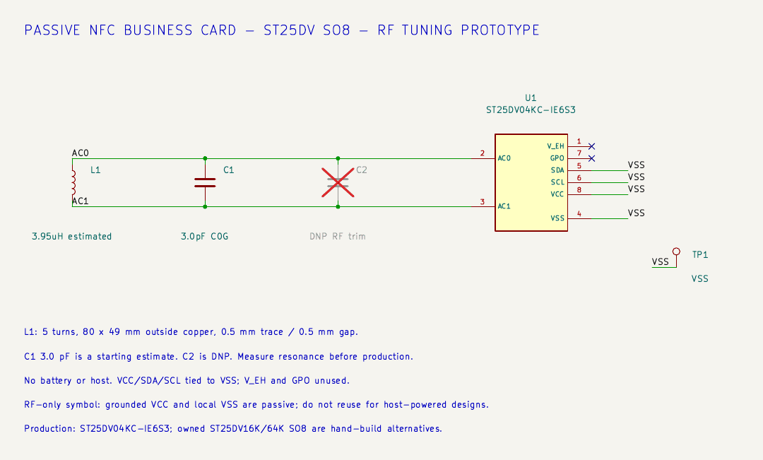
Antenna arithmetic that passed and was still rejected
The ST part has about 28.5 pF of input tuning capacitance. A three-turn 80 × 49 mm winding, roughly 1.64 µH by the usual rectangular-coil approximation, would resonate near target with about 51 pF outside the chip. An ST support reply on the ST community forum explains that a large low-loss external capacitor raises tag Q and can distort received modulation, and recommends keeping external capacitance below roughly 20% of the chip's, about 5.7 pF here. So the agents changed the winding, not the capacitor: five turns, about 3.95 µH, a theoretical 2.71 pF, and a stocked 3.0 pF part for a first-order prediction near 13.64 MHz. Chip tolerance alone spreads that to roughly 13.26–14.05 MHz, the 3 pF stray is assumed, the formula's exponent is empirical, and none of it is an EM simulation. Resonance arithmetic gives a starting value, not a working antenna.
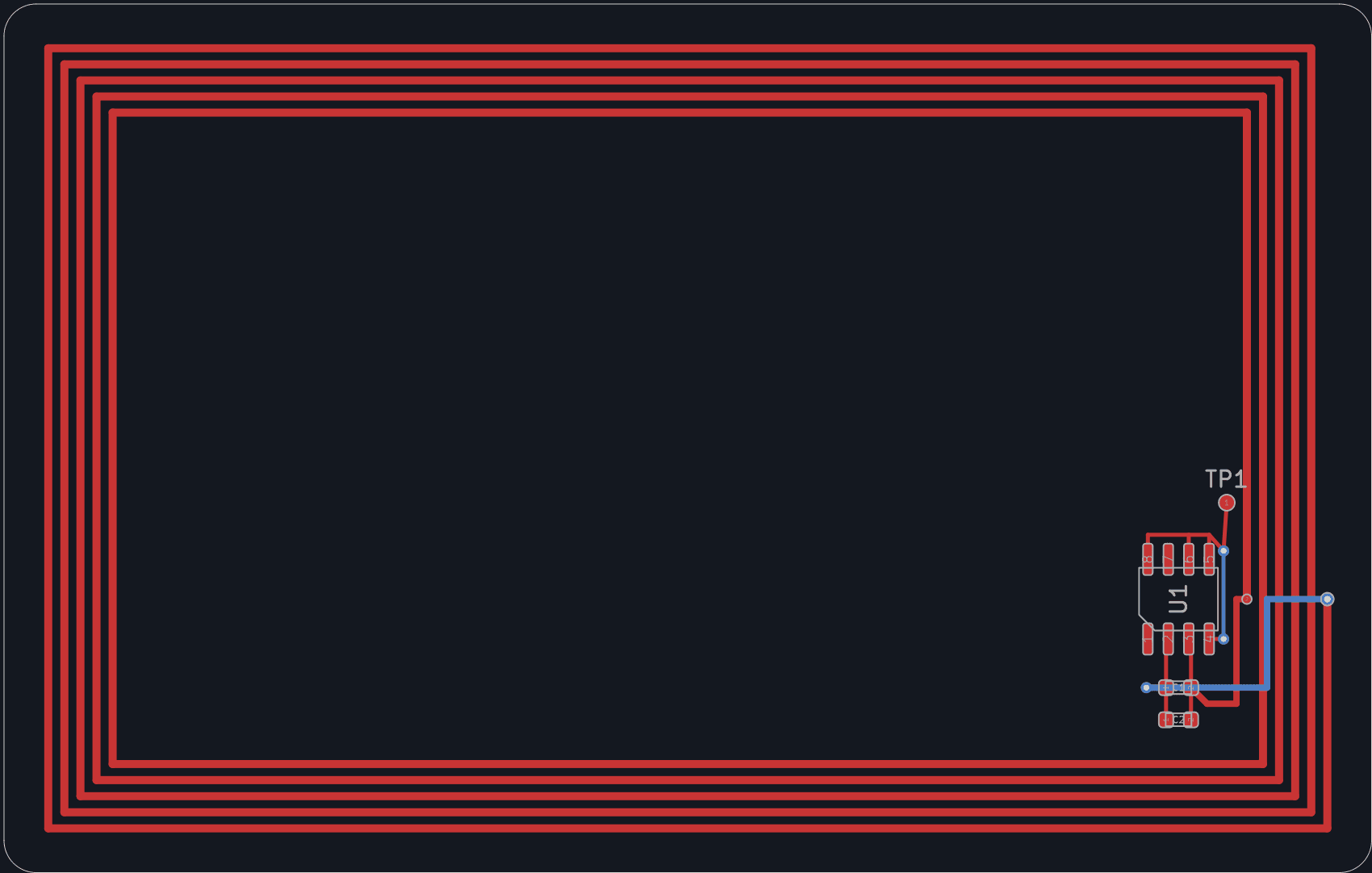
A printed antenna also needs explicit treatment in the files. The winding connects AC0 to AC1 at DC: drawn as ordinary tracks on two nets it looks like a short to DRC; drawn as graphics it has no connectivity at all. The generator represents it as a two-terminal schematic inductor with a footprint that declares a scoped net-tie between its two pads, so the exception covers the winding's intended connection and nothing else. An independent script then re-derives the coil from the exported front-copper Gerber rather than the generator's point list: 21 segments, 1,195 mm of centreline, 80 × 49 mm outside copper, a single unbranched path, 0.5 mm minimum non-adjacent gap. That proves exported geometry and continuity, not inductance, Q or read range.
Sourcing and assembly are part of the design loop
Assembly availability was researched before the layout was frozen, and it kept changing the board. The record keeps five channels apart: parts in my inventory; distributor retail stock; an assembler's catalog; stock allocated to an order; confirmed manufacturing and delivery dates. Only the first three exist here; no quote, upload, login, reservation or order happened.
The target service was LCSC's own PCBA offering, whose page stays on lcsc.com rather than redirecting to JLCPCB. LCSC exposed no part-level assembly inventory, so the agents separately inspected JLCPCB's public assembly catalog and API, which use the same component codes, and labelled that evidence as JLCPCB's. On 25 October, 22:34–22:39 Singapore time, the tag C3304276 showed 16,367 there, Extended and not Preferred; the 3.0 pF capacitor C46219 showed 144,328 with preferredComponentFlag: true. Observations, not reservations.
The fee vocabulary matters more than the stock numbers. Basic means no additional feeder or loading charge under the relevant policy, not a free component. Extended parts carry a fee per unique line: LCSC's FAQ says US$3 per unique Extended MPN; JLCPCB's table, updated 22 October, says US$3.07 for Economic assembly. Preferred Extended parts are exempt under JLCPCB's policy; whether LCSC honours that waiver for C46219 was not verified, so the quote could show roughly US$3 or US$6 in loading fees. Swapping the ordinary-Extended 2.7 pF candidate for the same-package 3.0 pF part kept one fee-bearing line without a footprint change; the swap was checked against the first-cut tuning range, moving the predicted centre only from 13.70 to 13.64 MHz. A few dollars is not a reason to change an RF value without review, so the 2.7 pF fallback stays documented.
The factory's published options then rewrote the physical spec. Black mask was offered only at 1.0 mm for 2–30 boards; 0.8 mm was green only; black with ENIG was not listed. So the early black, 0.8 mm, gold concept became 1.0 mm FR4, black mask, white silk, lead-free HASL, ten boards, top-side placement. And native DRC defaults did not enforce factory legibility: reference text was 0.8 mm with a 0.12 mm stroke; raising it to 1.0 mm and 0.15 mm made two capacitor labels overlap mask openings, which then had to move. A stricter constraint revealed a second, dependent problem.
Gerbers, BOM and CPL do different jobs: board geometry, exact part identities per reference, and fitted positions translated from KiCad's native export with no invented rotation correction. The supplier's placement preview showing pin 1 in the correct corner is still open.
A second chip, and an LED that proves power, not contact
A similar purpose does not make NFC chips interchangeable. On 26 October the agents built a separate NXP project rather than swapping the BOM; a hash check confirmed all 94 tracked ST files stayed byte-identical. The NXP part is the NT3H2111W0FHKH, NFC Forum Type 2 rather than Type 5, in a 1.6 × 1.6 mm XQFN8. The FHKH suffix selects that package; FT1X is SO8 and FTTJ is TSSOP8, and neither fits the footprint. The package drawings are a trap too: the datasheet's numbered top view and its underside view are mirrored, and the enlarged pin-1 land has to end up upper-left in the board's top view.
Its input capacitance is about 50 pF, not 28.5, so the same 80 × 49 mm outline wants three turns and a 20 pF capacitor for a prediction near 14.55 MHz, against NXP's 14.5 MHz single-tag target; the ST 20% rule was not imported, because NXP's own tuning guide retunes a coil with 100 pF. Unused host pins float, per NXP support, where the ST design grounds them. An independent review agent, parsing the netlist and copper separately from the generator, reported no file-level findings in revision A.
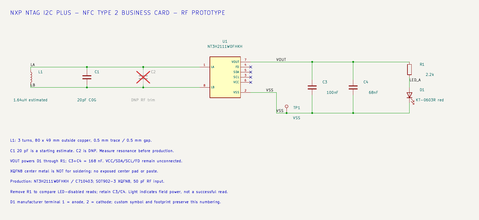
Revision B added the LED. NXP's energy-harvesting output can supply an external low-power load, so the circuit is VOUT through 2.2 kΩ into the LED and back to VSS, with 100 nF plus 68 nF as a local reservoir: 168 nF nominal against NXP's 150 nF typical and 220 nF maximum, though tolerance and X7R temperature drift stretch the real range to roughly 129–213 nF. The datasheet's typical phone example of 5 mA at 2 V is not a rating for this board, and more load means less communication margin, which is why revision A omitted the LED and why the resistor can be left off for an A/B comparison.
Two things only a careful reader catches. The LED's manufacturer numbers terminal 1 as the anode and 2 as the cathode, the opposite of KiCad's generic Device:LED, so the generator derives a project symbol and footprint that preserve the manufacturer numbering and says so in the coordinate notes. And the independent review of revision B raised the long reservoir return path; the capacitors moved directly under the IC, rotated 180°, and the route shortened to a loop of about 7.2 mm before the final export.
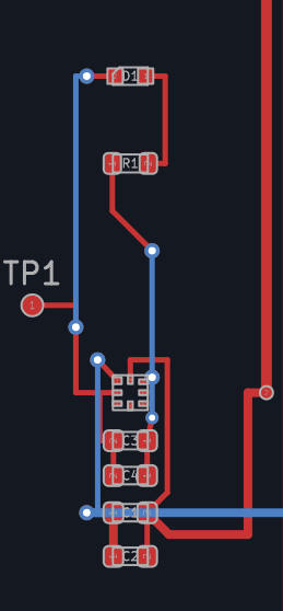
The LED revision's sourcing snapshot, 26 October 07:31 Singapore time, shows why the channels stay apart. The 100 nF reservoir capacitor C14663 showed 44,039,299 in JLCPCB's assembly catalog and zero in LCSC's retail inventory at the same check: a documented JLC assembly path, unconfirmed LCSC allocation, and no basis to infer that assembly stock can be bought loose. The four added parts cost about US$0.037 per board at JLCPCB catalog component prices, before attrition, placement, tax and other service charges, and were chosen Basic or Preferred Extended so the tag stays the only ordinary Extended line.
Artwork, generated and then made deterministic
The ST card's silkscreen motif came from the built-in image generator: a 1536 × 1024 monochrome field-line illustration, prompted as bold black ink on white with minimum stroke and gap widths. What went onto the board was a deterministic conversion: crop to ink bounds, threshold, resample at 0.15 mm pitch, a three-pixel opening to drop fragile tapered ends, then row run-lengths into 847 native silkscreen rectangles about 51 × 20.1 mm. No artwork touches copper, because decoration inside the winding changes RF behaviour. The QR on the back is deterministic modules at 0.48 mm, and ZXing decoded the URL from the native bottom render.

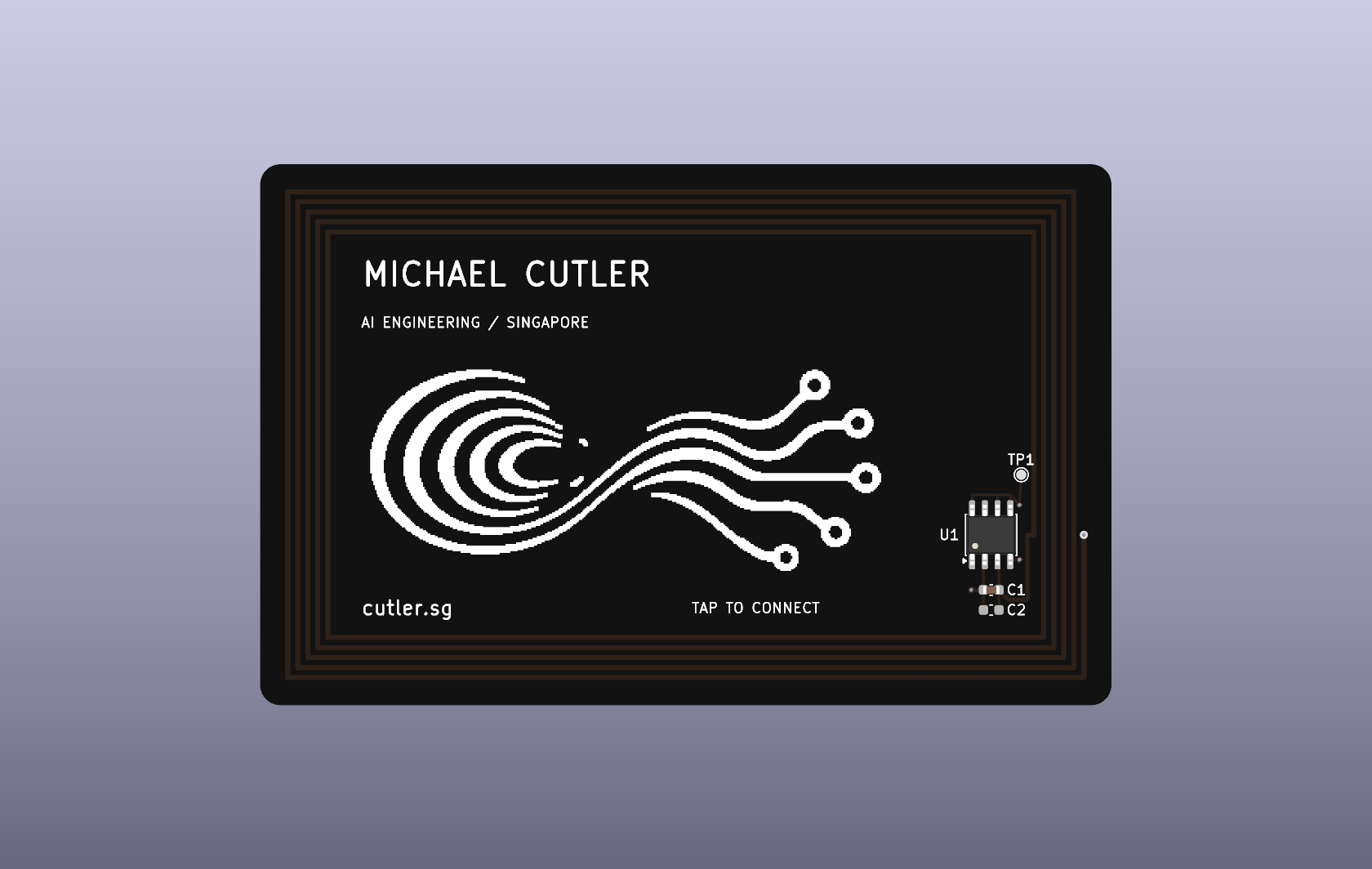
The last exploration asked what happens when the components and their traces become part of the composition. From revision B's six fitted parts, the agents proposed five directions and generated a mockup for each. These are visual proposals, not new boards: the images exaggerate package sizes and glow, draw the 1.6 mm XQFN as a large leaded package, and invent electrical details that must not be traced into copper. The brown perimeter rings are not antenna turns.
AI-generated art concepts — not routed PCBs
The Firefly pair is the useful before-and-after: the first image put the antennae at the lit end, so the LED read as a head; a targeted edit moved them to the lower end and the light became the abdomen. Attractive generated images depict wrong packages, wrong routes and wrong anatomy with equal confidence, which is why the lighthouse ranked first: it asks the least of the checked layout.
What is established, what isn't, and what I'd do next
Established: three native, editable KiCad designs exist, with project-local libraries. For each documented revision, ERC, DRC with schematic parity and unconnected-item counts are zero, with default-ignored categories listed rather than hidden and no blanket short-circuit waiver. Independent scripts re-checked pin topology against the datasheets, walked the exported Gerber winding, round-tripped the NDEF payloads and decoded the QR from the native render. Gerbers, drill, STEP, an assembly BOM and a CPL were generated and hashed; packaging refuses to zip anything whose hash drifted after validation. Dated supplier evidence was collected. The LED and the art concepts went through documented, reviewed iterations.
Not established: physical NFC read or write reliability; measured resonance, Q or read range; LED brightness or startup on real phones; assembly yield; a supplier's acceptance of these exact files; reserved stock or lead time; any order, delivery or assembled board. The default payload opens a URL; it does not save my contact details to anyone's phone. A clean ERC and DRC report is a statement about files. A lit LED would be evidence of harvested power, nothing more.
The remaining tests are the ones I'd have had to do anyway: fabricate a small batch on the final stack, measure resonance with a weakly coupled loop before and after fitting the tuning capacitor, then run repeated app-free reads and write-and-read-back cycles on the actual phones, with the LED fitted and with the resistor omitted.
What I'd keep is the shape of the workflow. Freeze the exact MPN, package suffix and pad numbering before anyone routes. Read inventory and the assembler's catalog early, and never let a retail count stand in for an allocation. Let the tool supply net names and let a separate script re-read what was exported. Treat a render as a claim to disprove. I did not time a manual baseline, so I cannot say how much time, if any, this saved.
Appendix: native outputs by revision
Native KiCad exports from each revision, or crops and rasterisations of them; the silkscreen preview comes from the artwork converter. Schematic and copper entries link to the SVG and PDF exports.
ST25DV04KC Type 5 card — commit 4a0d173, 25 October
NXP NT3H2111 card, revision A (no LED) — commit 36e0a2a, 26 October
NXP NT3H2111 card, revision B (field-powered LED) — commit c5a398e, 26 October
$ subscribe --newsletter
Practical AI engineering, in your inbox
Field notes for technical leaders building agents, evaluation systems, governance, and production infrastructure.
Related
When Should an Agent Ask Permission?
A useful agent acts within delegated authority, prepares consequential actions for review, and asks again when the action changes.
The 5-Step Loop: Why Your Agent Fails at Step 4
ReAct gave us a three-step loop. Production hardened it into five. The two new steps — Plan and Verify — are where everything that goes wrong, goes wrong. And the field has now named the worst offender.
The Gym Bot That Went to the App Store
I wrote a Claude Code skill in April because I book the same gym classes every week. By October it was an app on both stores, and an agent runs it. Here is why.